


- Profile of the company
- Technological limits
- Materials
- Term of delivery
- QM System
- Contact
- As to go to the CH-PRINT
CH-PRINT a.s.
Nám Dr. A. Schweitzera 194
916 01 Stará Turá
Slovak Republic
Tel: **421-(0)32-640 1361
032 640 1366
Mobil: **421-(0)905 563 413
Mobil: **421-(0)905 438 677
e-mail: ch-print@ch-print.sk
 |
Technological limits
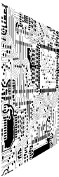
- Single-sided, double-sided or multilayer printed circuit boards
- Maximal format of panel 600 x 450 mm
- Minimal conductor spacing (gap):
- 0,12 mm (6 mil) for 18 µm thickness of copper foil
- 0,15 mm (8 mil) for 35 µm thickness of copper foil
- Minimal trace width (drawing width):
- 0,12 mm (6 mil) for 18 µm thickness of copper foil
- 0,15 mm (8 mil) for 35 µm thickness of copper foil
- Minimal pad – diameter of hole +0,2 mm (for 18 µm thickness of copper foil) (annular width 0.12 mm)
- Minimum drill diameter 0,2 mm (plated through holes -Aspect Ratio 1:10)
- Minimal overlap of photosensitive solder resist 0,2 mm (8 mil)
- Minimal overlap of 2 component solder resist 0,4 mm (16 mil)
- Minimal drawing width of legend 0,2 mm (8 mil)
- Cooper laminate thickness: 18, 35, 70, 105 µm
- Adjusting to final dimension:
- Milling – min. thickness of boards 0,3 mm (tolerance ±0,2 mm)
- Scoring – min. thickness of boards 0,6 mm (tolerance ±0,25 mm)
- shearing
- Electrical test by Fly Probe tester (Mania Loc8)
Notice:
It is possible to order min. quantity of boards which are equivalent 1 technological panel of format 130 x 70 mm).
peaty © 2007, CH-PRINT a.s. | Design by peaty